The future of computing requires advanced research in semiconductors today
IBM and its partners are inventing what’s next in semiconductors.
IBM and its partners are inventing what’s next in semiconductors.
Perhaps no invention has had a more profound impact on the direction of modern history than the transistor. Semiconducting transistors were integrated into circuits, which led to the creation of computer chips. Today, no aspect of our lives is untouched by semiconductors, and over the decades, chips have become smaller and faster — exponentially increasing the amount of processing power available to us.
The birth of the internet fundamentally changed how we use semiconductors; they no longer just power our computers — they’re integral to almost every aspect of our connected lives. A regular sedan car can have thousands of semiconductors in it. Entire businesses are run off smartphones. A pair of AirPods are more powerful than the computers we originally used to send astronauts to the Moon. Without access to increasingly powerful chips, our world would grind to a halt.
With the explosion of AI breakthroughs, the demand for powerful processing machines is soaring, along with new modalities to fit new use cases. For progress to continue in semiconductors, we need new approaches, new architectures, new materials — and new collaborations. We need a semiconductor industry fit for all of tomorrow’s challenges and burgeoning new platforms, like watsonx.
IBM has been pushing the computer industry forward as long as there’s been one. And when something didn’t exist, we made it — from the creation of electronic design automation (EDA), to the computers that powered those same astronauts to the Moon in the Apollo missions. In recent years, our breakthroughs have led to the 7 and 5 nanometer node chips that run many of today’s most advanced applications. We’ve designed new chips for new applications for our z Systems, such as the Telum processor, which brought powerful AI processing with milliseconds latency to IBM z16.
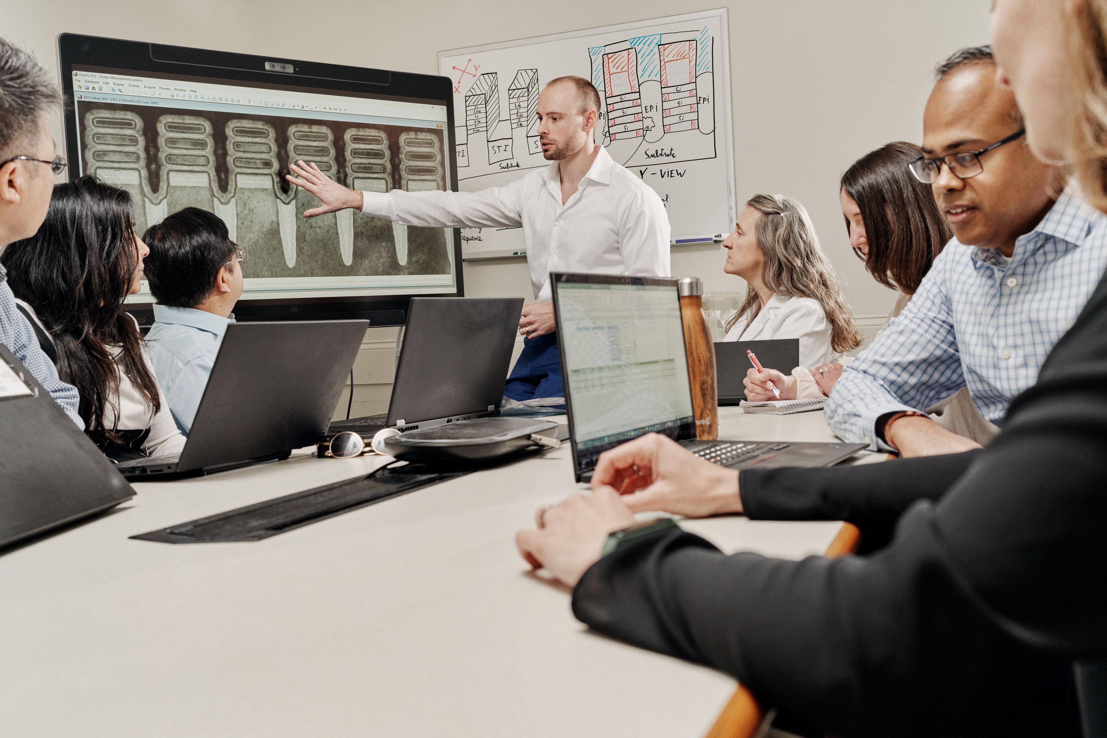
While we now partner for volume manufacturing, IBM has continued to lead the world in semiconductor breakthroughs, designing chips that are smaller, more powerful, and more energy efficient — like the nanosheet device structure, vertical transistors (VTFET), the world’s first 2 nanometer node chip, and the Artificial Intelligence Unit (AIU). Our focus today covers every aspect of semiconductors — including logic scaling, advanced chip packaging, and chiplet technologies — as well as new computing paradigms, like hybrid cloud, quantum computing, and AI.
And to truly realize the potential of the dawning age of AI, we believe that deeper levels of co-operation and innovation will be required. Over the years, chip production has become heavily centralized and supply chains have become brittle. At IBM Semiconductors, we’re also helping enable a balanced supply chain for computer chips, with investment, research, and partnerships in North America — and with key collaborators around the world.
We are in a renaissance for chip design, and at IBM Semiconductors, we’re focusing on bringing partners along for this journey. The specialization of the semiconductor industry is now so great that adding external partners into a shared platform for innovation could vastly accelerate innovation and production.
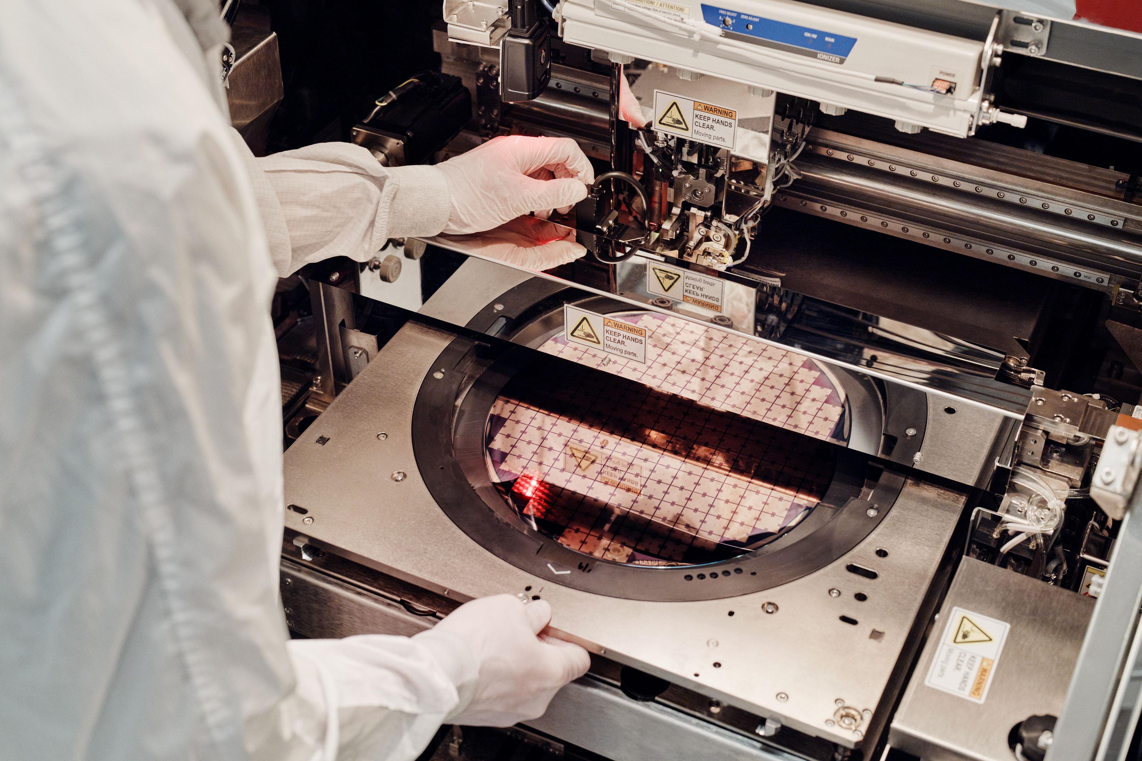
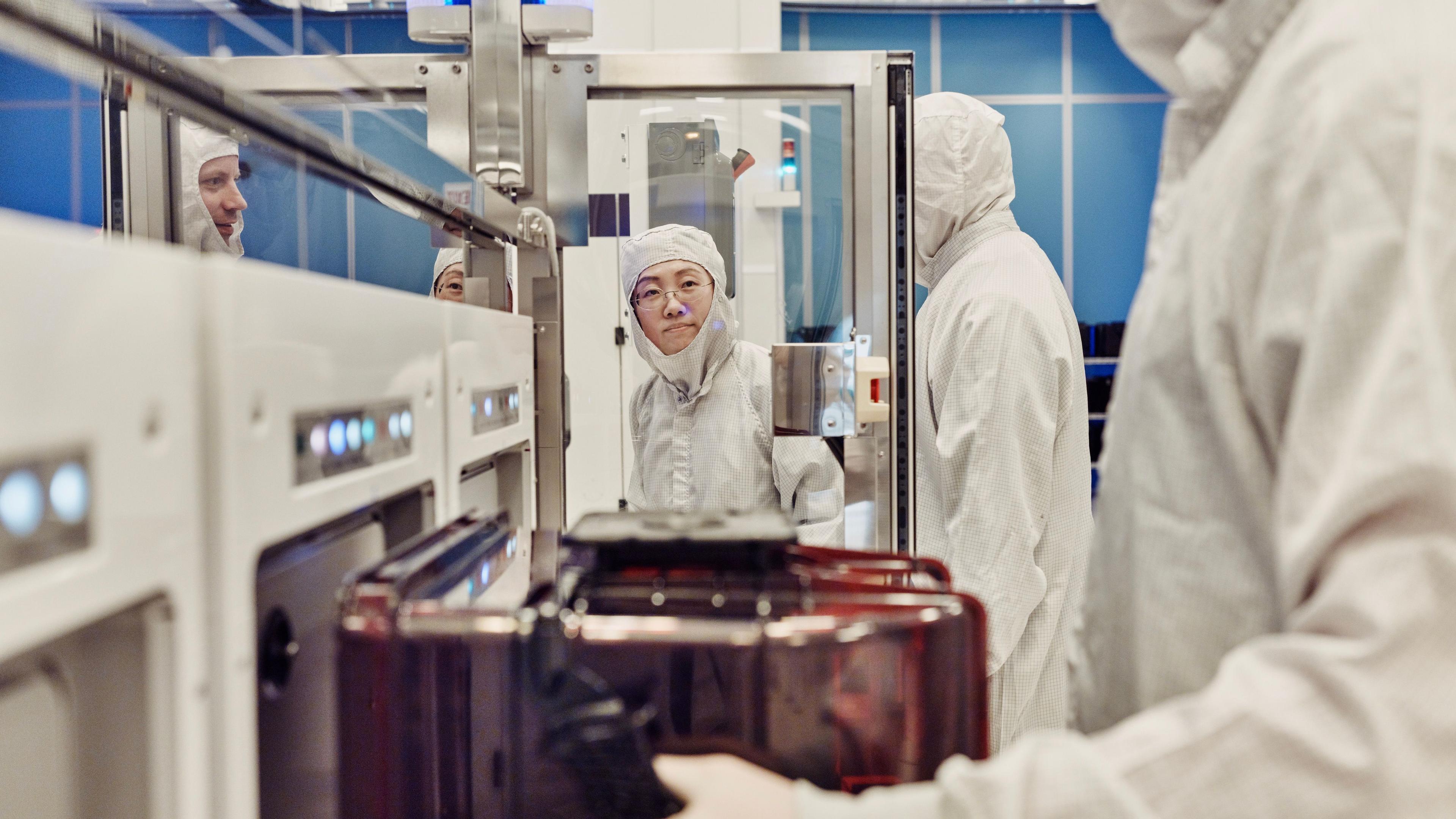
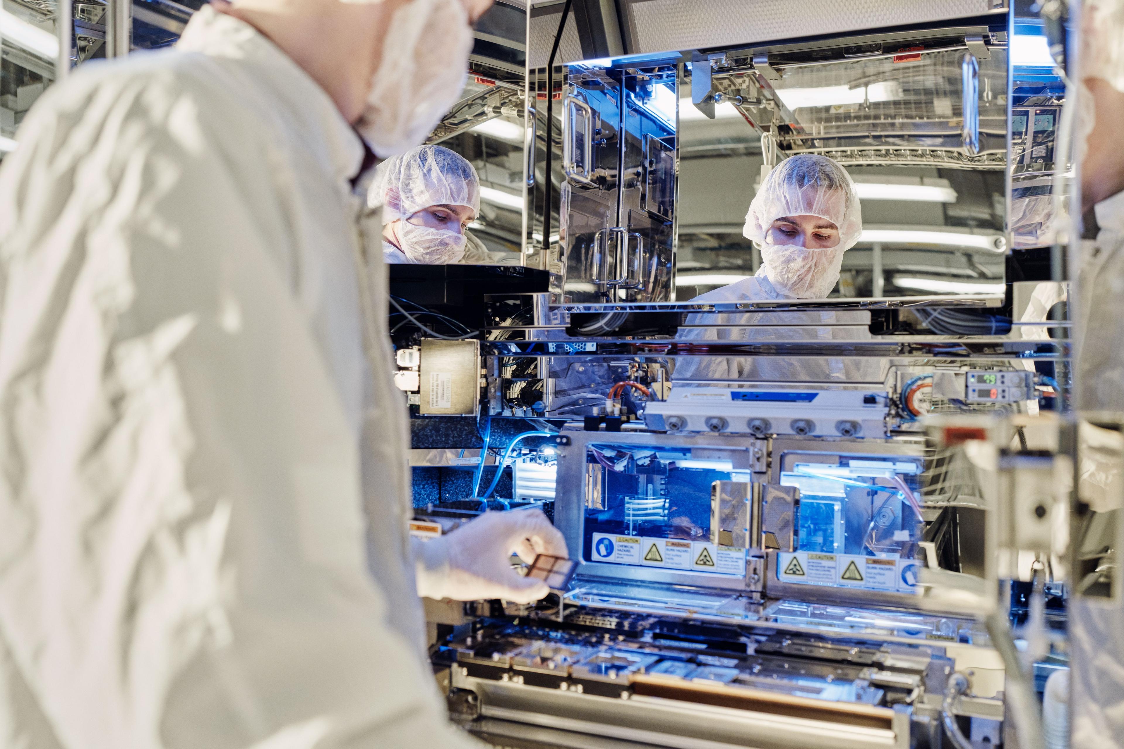
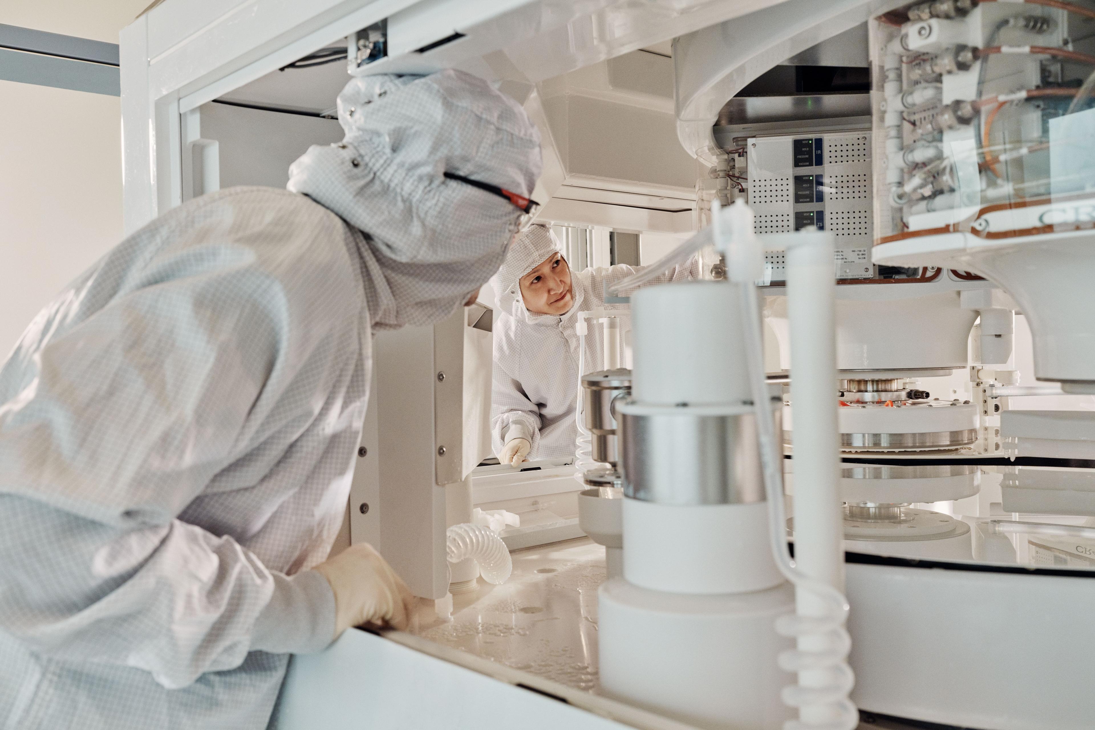
At our research facility in Albany, New York, we work alongside partners like Tokyo Electron, the State University of New York, and Samsung to invent solutions together for today’s most pressing device challenges.
IBM Research Albany is part of the Albany Nanotech Complex, the world’s leading ecosystem for semiconductor research, with a facility that spans five buildings and includes more than 100,000 square feet of semiconductor fab space. Many of the industry’s biggest breakthroughs in recent years have come out of this building, including our 2 nm node chips. The complex also houses one of the world’s most advanced photolithography systems, ASML’s Extreme Ultraviolet (EUV) lithography tool, which was critical to enabling the significantly higher density of transistors required for the 2 nm breakthrough.
With our partners, we’ve created a hub that combines the strengths of industry, government, and academia to drive faster progress and new breakthroughs. We believe this unique research environment in Albany could serve as a foundation for the proposed National Semiconductor Technology Center (NSTC), a key provision included in the bipartisan CHIPS and Science Act signed by President Biden last summer.
Albany is just one of the cutting-edge facilities in the IBM Semiconductors ecosystem — there’s also groundbreaking work being carried out in New York state at IBM Research’s headquarters in Yorktown Heights, as well as our facility in Poughkeepsie, and our advanced packaging manufacturing plant in Bromont, Canada.
With our Bromont facility, we have the opportunity to strengthen semiconductor packaging manufacturing capabilities and resiliency for North American supply chains. Advanced packaging is a crucial component of the semiconductor industry, and IBM’s Bromont plant has led the world in this process for decades. It’s one of North America’s largest chip assembly and testing facilities, having operated in the region for over 50 years. IBM is also working with the local government of Quebec at Bromont on the future of quantum computing, AI, and semiconductors research and development.
By bringing manufacturing and advanced packaging design back to North American shores, we believe we will see technological advances, economic growth, and enhanced security for the North American semiconductor ecosystem. But our vision for the future of semiconductors is not reliant on a single state or organization, but rather an open chiplet ecosystem that brings groups together to create opportunities for close collaboration, education, and innovation.
This is why IBM is expanding its partnership model and providing access to our unparalleled semiconductor research, expertise, world-class technology, and facilities — from invention to implementation. Research into semiconductors today is driving the breakthrough technologies that are shaping the future of chips, empowering the innovators of tomorrow.