IBM Research’s newest prototype chips use drastically less power to solve AI tasks
In a paper published in Nature today, IBM showed it’s possible to build analog AI chips that can handle natural-language AI tasks with an estimated 14 times more energy efficiency.

In a paper published in Nature today, IBM showed it’s possible to build analog AI chips that can handle natural-language AI tasks with an estimated 14 times more energy efficiency.
Although we’re still just at the precipice of the AI revolution, artificial intelligence has already begun to revolutionize the way we live and work. There’s just one problem: AI technology is incredibly power-hungry. By some estimates, running a large AI model generates more emissions over its lifetime than the average American car.
The future of AI requires new innovations in energy efficiency, from the way models are designed down to the hardware that runs them. And in a world that’s increasingly threatened by climate change, any advances in AI energy efficiency are essential to keep pace with AI’s rapidly expanding carbon footprint.
And one of the latest breakthroughs in AI efficiency from IBM Research relies on analog chips — ones that consume much less power. In a paper published in Nature today,1 researchers from IBM labs around the world presented their prototype analog AI chip for energy-efficient speech recognition and transcription. Their design was utilized in two AI inference experiments, and in both cases, the analog chips performed these tasks just as reliably as comparable all-digital devices — but finished the tasks faster and used less energy.
The concept of designing analog chips for AI inference is not new — researchers have been contemplating the idea for years. Back in 2021, a team at IBM developed chips that use Phase-change memory (PCM) works when an electrical pulse is applied to a material, which changes the conductance of the device. The material switches between amorphous and crystalline phases, where a lower electrical pulse will make the device more crystalline, providing less resistance, and a high enough electrical pulse makes the device amorphous, resulting in large resistance. Instead of recording the usual 0s or 1s you would see in digital systems, the PCM device records its state as a continuum of values between the amorphous and crystalline states. This value is called a synaptic weight, which can be stored in the physical atomic configuration of each PCM device. The memory is non-volatile, so the weights are retained when the power supply is switched off.phase-change memory to encode the weights of a neural network directly onto the physical chip. But previous research in the field hasn’t shown how chips like these could be used on the massive models we see dominating the AI landscape today. For example, GPT-3, one of the larger popular models, has 175 billion parameters, or weights.
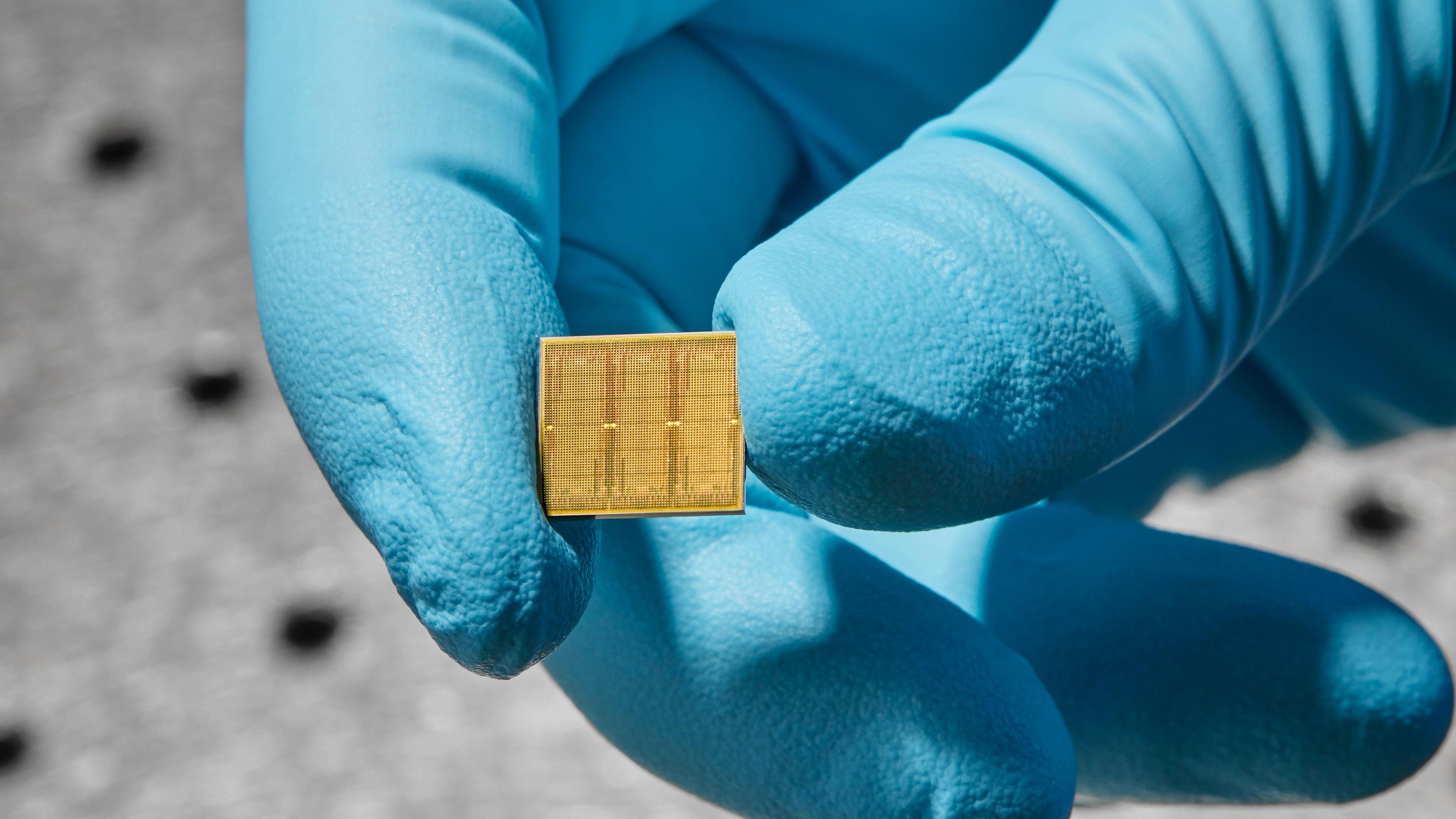
The design that the team at IBM Research have created can encode 35 million phase-change memory devices per chip; in other words, models with up to 17 million parameters. While this isn’t yet at a size comparable to today’s cutting-edge generative AI models, combining several of these chips together has allowed it to tackle experiments on real AI use cases as effectively as digital chips could.
The approach the team took was to optimize the In computing, and especially in digital signal processing, a MAC operation is when the the product of two numbers is computed and added to an accumulator, part of the CPU that deals with arithmetic in process. MACs are a fundamental computing unit.multiply-accumulate (MAC) operations that dominate deep-learning compute. By reading the rows of an array of resistive non-volatile memory (NVM) devices, and then collecting currents along the columns, the team showed they can perform MACs within the memory. This eliminates the need to move the weights between memory and compute regions of a chip, or across chips. The analog chips can also carry out many MAC operations in parallel, which saves time and energy.
The concept of analog has tremendous potential, but there are also significant challenges for chip design and manufacturing: Analog computing is inherently imprecise, new processes will have to be developed to produce high-yield NVMs at scale, and for connecting analog chips to traditional digital systems. But the work researchers at IBM have carried out points to a future where these chips could potentially be as useful as digital chips.
The team at IBM Research devised two experiments to test out the efficacy of their designs. The first one revolved around keyword utterance detection. In the way that you would expect your smart speaker to respond if you said, “Hey Siri” or “Hey Google” out loud, the team wanted to see they could use their chip design to recognize specific spoken words. They built a system that listened for 12 words, and in each case, the analog chip could react to each word with the same accuracy as the software-based systems that exist today — but considerably faster. The systems that wait and listen for a specific keyword today require power to sit idly waiting, whereas the design the team created can be powered down when not needed, since the model weights are stored on-chip, in non-volatile memory.
Using models uploaded to MLCommons, an industry benchmarking and collaboration site, the team could compare their demo system’s efficacy to those running on digital hardware. Developed by MLCommons, the MLPerf repository benchmark data showed that the IBM prototype was seven times faster over the best MLPerf submission in the same network category, while maintaining high accuracy. The model was trained on GPUs using hardware-aware training and then deployed on the team’s analog AI chip.
The second experiment was considerably larger, and hints at a future where generative AI systems, built on analog chips, could be used in place of digital ones. It aimed to implement a large, complex model, using five of the team’s chips stitched together, and simulated off-chip digital computations to showcase the scalability of analog AI. The researchers ran a recurrent neural network transducer (or RNNT) speech-to-text model found on MLPerf to transcribe, letter by letter, what a person is saying. RNNTs are popular for many real-world applications today, including virtual assistants, media content search and subtitling systems, and clinical documentation and dictation.
The system contained 45 million weights on 140 million PCM devices across five chips. It was able to take audio of people speaking and transcribe it with an accuracy very close to digital hardware setups. Unlike the first demo, this one was not entirely end-to-end, meaning it did require some off-chip digital computation. However, so little additional compute is involved here that, had it been implemented on the chip, the resulting energy efficiency would still be higher than products on the market today.
Once again using data uploaded to MLCommons, the team compared their network’s efficacy to RNNTs running on digital hardware. MLPerf data showed that the IBM prototype was estimated to be roughly 14 times more performant per watt — or efficient — than comparable systems. This is the first analog system that IBM researchers have been able to actually test with MLPerf, as past experiments have just been too small to compare.
Natural-language tasks aren’t the only AI problems that analog AI could solve — IBM researchers are working on a host of other uses. In a paper published earlier this month in Nature Electronics, the team showed it was possible to use an energy-efficient analog chip design for scalable mixed-signal architecture that can achieve high accuracy in the CIFAR-10 image dataset for computer vision image recognition.
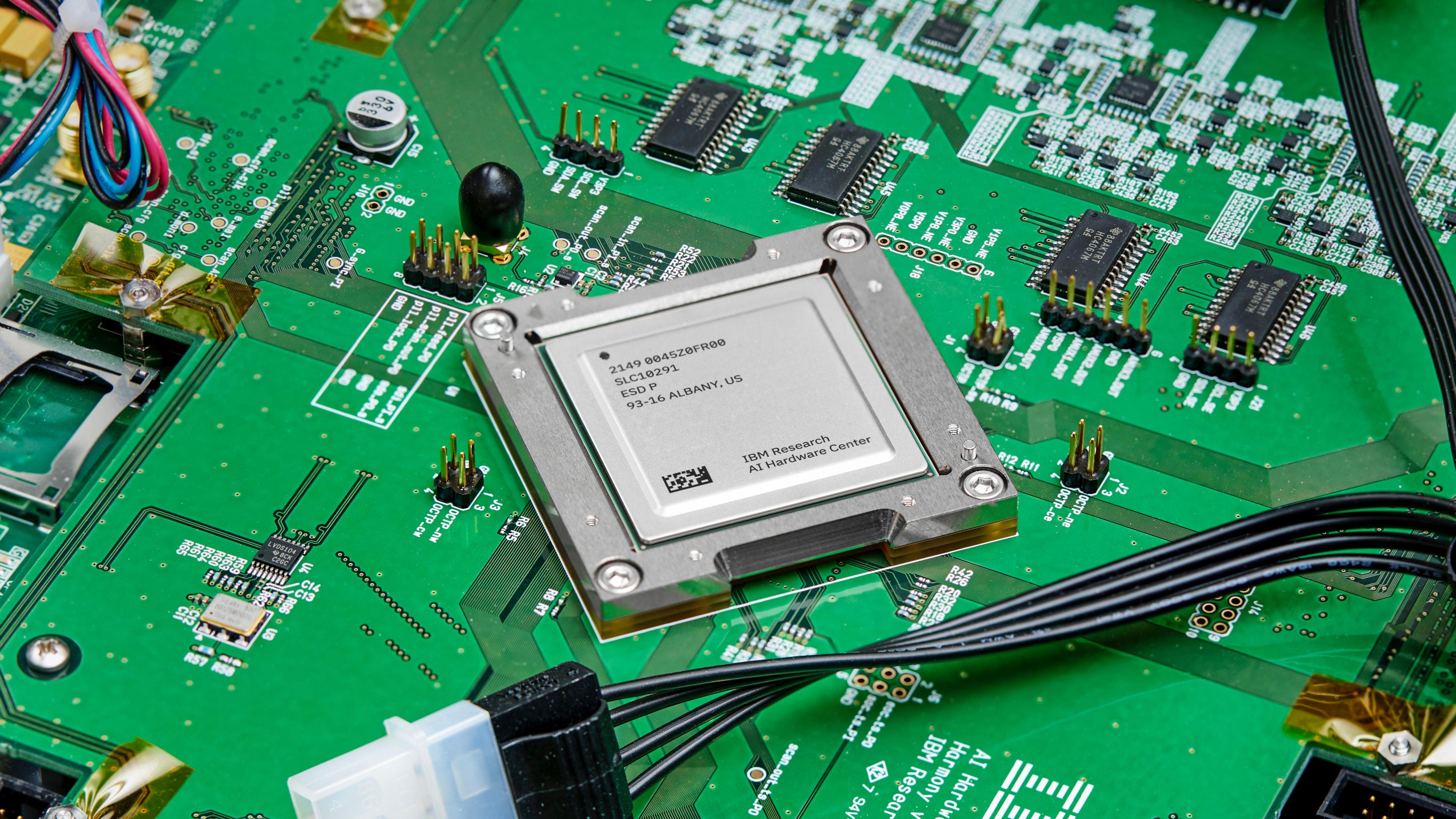
These chips were conceived and designed by IBM researchers in the Tokyo, Zurich, Yorktown Heights, New York, and Almaden, California labs, and built by an external fabrication company. The phase change memory and metal levels were processed and validated at IBM Research’s lab in the Albany Nanotech Complex.
If you were to combine the benefits of the work published today in Nature, such as large arrays and parallel data-transport, with the capable digital compute-blocks of the chip shown in the Nature Electronics paper, you would see many of the building blocks needed to realize the vision of a fast, low-power analog AI inference accelerator. And pairing these designs with hardware-resilient training algorithms, the team expects these AI devices to deliver the software equivalent of neural network accuracies for a wide range of AI models in the future.
While this work is a large step forward for analog AI systems, there is still much work to be done before we could see machines containing these sorts of devices on the market. The team’s goal in the near future is to bring the two workstreams above into one, analog mixed-signal, chip. The team is also looking to see how foundation models could be implemented on their chips.
Analog AI is now very much on the path to solving the sorts of AI problems that today’s digital systems are tackling, and the vision of power-conscious analog AI, married up with the digital systems we use today, is becoming clearer.
Date
23 Aug 2023Notes
- Note 1: Phase-change memory (PCM) works when an electrical pulse is applied to a material, which changes the conductance of the device. The material switches between amorphous and crystalline phases, where a lower electrical pulse will make the device more crystalline, providing less resistance, and a high enough electrical pulse makes the device amorphous, resulting in large resistance. Instead of recording the usual 0s or 1s you would see in digital systems, the PCM device records its state as a continuum of values between the amorphous and crystalline states. This value is called a synaptic weight, which can be stored in the physical atomic configuration of each PCM device. The memory is non-volatile, so the weights are retained when the power supply is switched off. ↩︎
- Note 2: In computing, and especially in digital signal processing, a MAC operation is when the the product of two numbers is computed and added to an accumulator, part of the CPU that deals with arithmetic in process. MACs are a fundamental computing unit. ↩︎
References
-
Ambrogio, S., Narayanan, P., Okazaki, A. et al. An analog-AI chip for energy-efficient speech recognition and transcription. Nature 620, 768–775 (2023). ↩