- Rudy J. Wojtecki
- Magi Mettry
- et al.
- 2018
- ACS AMI
Semiconductor fabrication & packaging
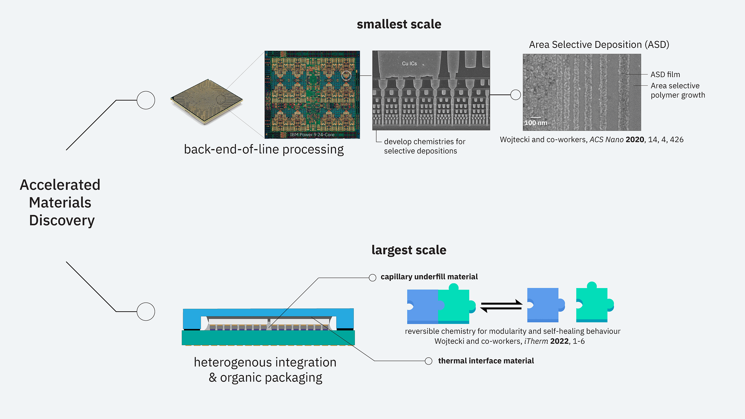
We’re developing new materials for both the smallest length scale (<20nm) and largest length scale (>20mm) of semiconductor fabrication.
Overview
Smallest length scale (<20nm):
The advancement of electronic technologies are largely dependent on patterning materials, such as polymer resists and subtractive processes to create desired features and continue to extend the capabilities of nanoscale fabrication at a remarkable rate. Lithography underpins this ability and remains the cornerstone for device fabrication. As the demand for ever-increasing densities in energy storage & capture, medical device advances and computational scaling rises, the development and maturation of bottom-up additive strategies has become increasingly more important. Atomic Layer Deposition (ALD) is a bottom-up technique that enables exquisite layer-by-layer control of film compositions. This method of film generation relies on efficient chemical reactions at a surface wherein two self-limiting half reactions are alternated to produce conformal thin films even on high-aspect ratio features and three-dimensional structures. The reliance on self-limiting reactions provides a high degree of control over the deposited material thickness and composition. These reactions can also be inhibited in a controllable area selective manner, which provides a critical means of depositing a film without a lithographic or subtractive process. This method, often referred to as Area Selective Deposition (ASD), is of significant economic value as device scaling encounters increasingly difficult challenges in wiring nanoscale devices to the outside world, where sensitivity to variations in the alignment of multiple lithography steps grows dramatically (e.g., overlay errors). Often when an overlay error occurs, this results in device connections (wiring) away from their target placement and form in closer proximity to other device features, leading to parasitic capacitance, higher localized temperature, lower yield and device variability. Self-aligned selective deposition can relax these overlay requirements by introducing surface topography and downstream requirements to enable processes such as fully aligned via for a commercially relevant implementation. Novel device architectures are drawing from a wider variety of non-traditional fabrication methods to produce three dimensional structures such as resistive random access memory (RRAM) that makes use of 3D cross point arrays for AI hardware devices. This increases the challenge for traditional fabrication processes and further motivates the development of bottom-up depositions capable of spatial control in three dimensions and on surface topography (e.g. corners, sharp bends and line-edges). Our work is focused on the synthesis of selective surface-binding inhibitors to enable area selective processes and provide a more complete understanding of inhibitor structure/property relationships.
Largest length scale (>20mm):
As the physical complexity of multi-chip modules (MCMs) and demand for improved thermal management increases, traditional electronic packaging materials may reach fundamental limitations. For instance, capillary underfills when subjected to thermal stresses from typical operating temperatures are susceptible to fatigue, crack formation, adhesion loss and related failure mechanisms – all of which have significant consequences to package lifetime and performance. In general, packaging materials are complex formulations that include filler, matrix polymers, catalysts and adhesion promoters. The curing chemistry is reliant on an irreversible bond formation (often thermosetting epoxy resins) where efforts are directed to minimize the rupture of these bonds. The incorporation of chemical moieties capable of bond formation under an equilibrium (e.g., reversible bond formation) provides access to macroscopic behaviors such as mechanophores, shape-memory behavior and autonomic self-healing. By judicious selection of dynamic bonds, multiple material responses can be generated by orthogonal stimuli. With an eye towards wide ranging electronic packaging applications, a dual responsive material system was synthesized that exhibits both autonomic re-healing properties, triggered by a thermal stimulus, and re-workability from a chemically triggered depolymerization. These are attractive properties for packaging materials as they can extend the lifetime of the material through damage repair, offer a pathway for improved yields, and enable more complex MCMs through a facile chemical method of re-workability (e.g., depolymerization).