Boost your tools: Introducing ToolOps, the tool lifecycle extension in ALTK
Technical note
Himanshu Gupta, Jim Laredo, Neelamadhav Gantayat, Jayachandu Bandlamudi, Prerna Agarwal, Sameep Mehta, Renuka Sindhgatta, Ritwik Chaudhuri, and Rohith Vallam
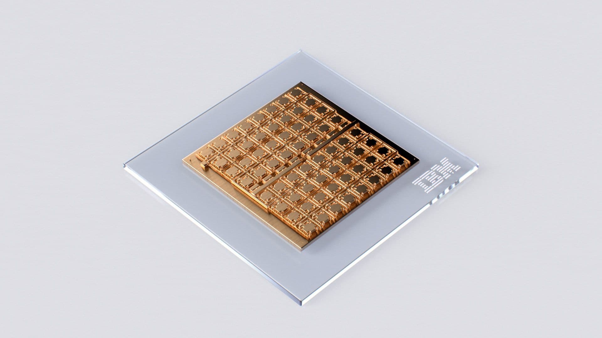
The energy-efficient chip showcases critical building blocks of a scalable mixed-signal architecture.
We’re just at the beginning of an AI revolution that will redefine how we live and work. In particular, deep neural networks (DNNs) have revolutionized the field of AI and are increasingly gaining prominence with the advent of foundation models and generative AI. But running these models on traditional digital computing architectures limits their achievable performance and energy efficiency. There has been progress in developing hardware specifically for AI inference, but many of these architectures physically split the memory and processing units. This means the AI models are typically stored in a discrete memory location, and computational tasks require constantly shuffling data between the memory and processing units. This process slows down computation and limits the maximum achievable energy efficiency.
IBM Research has been investigating ways to reinvent the way that AI is computed. Analog in-memory computing, or simply analog AI, is a promising approach to address the challenge by borrowing key features of how neural networks run in biological brains. In our brains, and those of many other animals, the strength of synapses (which are the “weights” in this case) determine communication between neurons. For analog AI systems, we store these synaptic weights locally in the conductance values of nanoscale resistive memory devices such as Phase-change memory (PCM) works when an electrical pulse is applied to a material, which changes the conductance of the device. The material switches between amorphous and crystalline phases, where a lower electrical pulse will make the device more crystalline, providing less resistance, and a higher electrical pulse makes the device more amorphous, resulting in more resistance. Instead of recording the usual 0s or 1s you would see in digital systems, the PCM device records its state as a continuum of values between the amorphous and crystalline states. This value is called a synaptic weight, which can be stored in the physical atomic configuration of each PCM. The memory is non-volatile, so the weights are retained when the power supply is switched off.phase-change memory (PCM) and perform multiply-accumulate (MAC) operations, the dominant compute operation in DNNs by exploiting circuit laws and mitigating the need to constantly send data between memory and processor.
To turn the concept of analog AI into a reality, two key challenges need to be overcome: These memory arrays need to be able to compute with a level of precision on par with existing digital systems, and they need to be able to interface seamlessly with other digital compute units, as well as a digital communication fabric on the analog AI chip.
In a paper published today in Nature Electronics, IBM Research made a significant step towards addressing these challenges by introducing a state-of-the-art, mixed-signal analog AI chip for running a variety of DNN inference tasks. It’s the first analog chip that has been tested to be as adept at computer vision AI tasks as digital counterparts, while being considerably more energy efficient.
The chip was fabricated in IBM’s Albany NanoTech Complex, and is composed of 64 analog in-memory compute cores (or tiles), each of which contains 256-by-256 crossbar array of synaptic unit cells. Compact, time-based analog-to-digital converters are integrated in each tile to transition between the analog and digital worlds. Each tile is also integrated with lightweight digital processing units that perform simple nonlinear neuronal activation functions and scaling operations.
Each tile can perform the computations associated with a layer of a DNN model. The synaptic weights are encoded as analog conductance values of the PCM devices. A global digital processing unit is integrated in the middle of the chip that implements more complex operations that are critical for the execution of certain types of neural networks. The chip also has digital communication pathways at the chip interconnects of all the tiles and the global digital processing unit.
Using the chip, we performed the most comprehensive study of compute precision of analog in-memory computing and demonstrated an accuracy of 92.81% on the CIFAR-10 image dataset. We believe this to be the highest level of accuracy of any currently reported chips using similar technology. In the paper, we also showed how we can seamlessly combine analog in-memory computing with several digital processing units and a digital communication fabric. The measured throughput per area for Giga-operations per second (GOPS) by area is a standard metric for describing compute efficiency where raw compute operations are normalized by a concomitant compute area. It essentially shows that there are more operations for a given area, meaning this chip is a more efficient compute engine.8-bit input-output matrix multiplications of 400 GOPS/mm2 of the chip is more than 15 times higher than previous multi-core, in-memory computing chips based on resistive memory, while achieving comparable energy efficiency.
By combining the area- and energy-efficient analog-to-digital converters (ADCs), highly-linear multiply–accumulate-compute, and capable digital compute-blocks of this 64-tile chip with massively-parallel data-transport that we showed off in a 34-tile chip presented at the IEEE VLSI symposium in 2021, we now have demonstrated many of the building blocks needed to realize an architectural vision for a fast, low-power analog AI inference accelerator chip.
Using our learning we have designed an accelerator architecture like this which was published earlier this year in IEEE Transactions on VLSI systems. Our vision combines many analog in-memory computing tiles with a mix of special-purpose, digital compute-cores connected with a massively-parallel 2D mesh. In conjunction with sophisticated hardware-aware training we have developed in recent years, we expect these accelerators to deliver software-equivalent neural network accuracies across a wide variety of models in the years ahead.


